Category Archives: Engineering Perspectives

Atmel wireless connectivity supports industrial IoT revolution


The BTLC1000 exhibits the lowest BLE power consumption in the industry.


With both this year’s CES and Embedded World now behind us, it’ll be interesting to see which of the gadgets unveiled during these shows find a way to market — some will go to production, others won’t. I am skeptic about the smart shoe offering self-fastening mechanism… And during these two weeks, the IoT revolution has silently progressed in industrial automation. (You will be surprised if you read some very serious white papers extracted from the Internet of Things series published by Bosch.)

ble1000_google-banner.jpg

While attendees flocked to Vegas, progresses were made in industrial automation thanks to hard work being done in Germany. In fact, these two worlds — consumer oriented and industrial — are both relying on wireless connectivity, including products from Atmel: the ATWILC1000, ATWILC1500 or ATWILC3000 supporting Wi-Fi and ATBLC1000 supporting BTLE 4.1,which  was recently crowned “Product of the Year” from Electronic Products.

According to Bosch’s white paper “Leveraging the Internet of Things: Companies can streamline business processes for stakeholders across the extended enterprise,” we realize that Bosch’s managers have brainstormed about the IoT to extract the added business value for the enterprise, like for example, “in manufacturing, data automatically collected from smart and connected products, give companies meaningful feedback as to how products should be reengineered, and provides opportunities for additional revenue through selling services.”

In order to become smart and connected, industrial products need to integrate either a Wi-Fi connection supported by ATWINC1500, or a Bluetooth supported by the very tiny (see above) ATBTLC1000.

IoT-scalability-courtesy-Bosch

Shows the requirements for scalability on two current customer PoCs at Bosch Software Innovations. These PoCs start in year one with a very low umber of connected devices and sensors. However, in a short space of time, they scale massively upward for commercial launch and rollout.

From the above graphic, extracted from another white paper from Bosch, “Realizing the connected world-how to choose the right IoT platform,” we can derive two crucial information. The first is the fact that IoT is already a reality in the industrial market segment, not really known to be fashion driven like could be consumer electronic. The second information is about scalability. In both examples, the number of connected devices was very low, but in a short space of time they scale massively, reaching 500k devices for the first and up to 3 million for the other. A single industrial automation application can generate a very good semiconductor business, including sensors, MCU and wireless connectivity device. In our previous blog, we have investigated the ATWINCxx00 family bringing Wi-Fi connectivity to any embedded design. Let’s take a look at the award winner ATBTLC1000 device supporting BT 4.1 connectivity.

Atmel's BTLC1000

The BTLC1000 is an ultra-low power Bluetooth SMART (BLE 4.1) SoC with an integrated ARM Cortex-M0 MCU, a transceiver, a modem, MAC, PA, TR Switch, and a power management unit (PMU). It can be used as a BLE link controller or data pump with external host MCU, or as a standalone applications processor with embedded BLE connectivity and external memory. If we look at the key features list:

  • BLE4.1 compliant SoC and protocol stack
  • Lowest BLE power consumption in industry
  • Smallest BLE 4.1 SoC — Available in WLCSP (2.26×2.14mm) or QFN ( 32p 4×4 mm)
  • Optimized system cost — High level of integration on chip reduces external Bill of Material significantly
  • Wide operating Voltage range — 1.8 – 4.3V
  • Host Interface — SPI or UART
  • Certified modules — FCC, ETSI/CE, TELEC
  • Enterprise Development support & tools with the ATBTLC1000 Xplained Pro

The main reasons why the Atmel BTLC1000 has won the Electronic Design award are power, cost and certification. This chip not only exhibits the lowest BLE power consumption in the industry, it’s also the smallest BLE 4.1 SoC (see picture) offering optimized system cost, thanks to high level of integration. If companies like Bosch supporting industrial automation segment for years (if not centuries) start to be seriously involved into smart connected IoT systems, no doubt that ATBTLC1000 and ATWILC1000 devices have a bright future…


This post has been republished with permission from SemiWiki.com, where Eric Esteve is a principle blogger and one of the four founding members of the site. This blog first appeared on SemiWiki on January 10, 2016.

tinyAVR in 8- and 14-pin SOIC now self-programming


The ATtiny102/104 retain the AVR performance advantage — still a 12 MIPS core with 1KB Flash and 32B SRAM — and upgrade many of the features around it.


At this week’s Embedded World 2016, Atmel is heading back to 8-bit old school with their news, straight to the low pin count end of their MCU portfolio with a significant upgrade to the tinyAVR family.

According to Atmel’s briefing package, development of the ATtiny102 and ATtiny104 has been in progress for some time. We got a peek at the company’s roadmap for AVR where these are labeled “next generation tinyAVRs,” and all we can say is this is the beginning of a significant refresh — alas, we can’t share those details, but we can now look at these two new parts.

What jumps out immediately is how the AVR refresh fills a significant gap in Atmel’s capability. The existing tinyAVR family is anchored by the ATtiny10, a capable 8-bit AVR core running at up to 12 MIPS with 0.5 or 1KB Flash and 32B of SRAM. The pluses of extended availability are obvious at the beginning of the lifecycle, but by the midpoint of a long run, the technology can start to seem dated.

 ATtiny102/ ATtiny104

ATtiny102/ ATtiny104

That is certainly the case for the ATtiny10 introduced in April 2009. At that time, the ATtiny10 was a shot straight at the Microchip PIC10F, with much higher CPU performance and a competitive 6-pin SOT and 8-pin DFN package offering. Outside of the CPU itself, the ATtiny10 and PIC10F line up pretty closely except for two areas: self-programming, and the accuracy of on-chip oscillators and voltage references. ATtiny10 parts require pre-programming from Atmel or a distributor, and its rather wide accuracy specs need help from product calibration and external componentry – however, cost and code compatibility still have a lot of sway, and the popularity of the ATtiny10 was unshaken.

The ATtiny102/104 retain the AVR performance advantage — still a 12 MIPS core with 1KB Flash and 32B SRAM — and upgrade many of the features around it. First and most noticeable is a packaging improvement. The ATtiny102 comes in an 8-pin SOIC (with the 8-pin DFN option still available). For a generation of applications needing more I/O in a low-cost part, the ATtiny104 comes in a pin-compatible 14-pin SOIC with 6 extra I/O pins.

Features for ATtiny102/ ATtiny104

Self-programming of Flash has been added to both versions, and with the same core footprint a single production image for both parts is achievable. Fast start-up time is available as an option as well. The internal voltage references are now highly accurate, with calibrated 1.1V, 2.2V, and 4.3V taps at +/- 3%. Internal oscillator accuracy is now +/- 2% over a 0 to 50 degrees C temperature range at fixed voltage. Those changes prompted expanding successive approximation ADC resolution to 10-bit, and channels are doubled to eight. Two of the I/O pins can now be configured for a USART, adding serial communications capability. A new 10-byte Unique ID provides a serial number.

Those features translate to customer satisfaction with intelligent devices using the ATtiny102 and ATtiny104. The more accurate internal oscillator improves the precision of motor control in personal care devices such as toothbrushes and electric shavers. The calibrated voltage references enable applications where rechargeable battery management is a primary function, for example in the d.light family of portable solar-powered lighting.

For more information on the ATtiny102 and ATtiny104 MCUs, you can check out Atmel’s recent post here.

This announcement, and what I think will follow from Atmel later this year, reaffirms just how important 8-bit is for the future at Atmel. The AVR architecture is beloved because of its simplicity and ubiquity with over 7B cores now shipped. The advances in the ATtiny102 and ATtiny104 are aimed at reducing BOM and manufacturing costs and enabling further innovation in intelligent consumer devices.

Digital audio recording “you” with quality and ease


Instamic wants to do for microphones what the GoPro did for cameras. 


Many analog years ago, digital recorded audio won the popularity contest. Nowadays, whether it’s from your mobile phone, infotainment system or personal audio device, every sound you hear is from digitally encoded bits.

Digital audio has eliminated all of the analog audio’s distortions and noise-related problems. Quite simply, people are shaped and drawn to recorded audio, ranging from music producers, to creative artist, to the everyday consumer. It’s in these moments for the user, high-quality audio conveys clarity in the recording moments. In today’s user interfaces, from media and podcasts to tablets, many whizzing bits are streaming a world of information including audio — readily available at every reach of a finger or ear.

The Miracle of Sound all Around US

More and more, we are seeing the prolific expansion and seamless integration of the stack. What does this all mean, though? Screen time now captivates us, while voice recognition and audio are blended into the user pathways of UX. Spurring from technology, we see popular apps like Evernote and iOS/Android natively adopting audio recording right within its inherent interface. These apps are taking in the voice user input to also drive UX — cleverly weaving experience, intention, outcome, commenting and moments.

Almost every sound you hear coming out of a speaker is digitally sampled and encoded.  Moment upon moment of keynotes stored are recorded more, albeit in the format of video or audio, we are seeing an increasing number of unique use cases to why one would want to capture a particular moment. These moments offer an on-demand periscope — referencing a historic timeline of ripples in our experience, memory, and journey through work, life, play, and what matters most to us.

referencing a historic timeline of ripples in our experience

For much of our pleasures, sound is always in digital — whether it’s on your smartphone, computer, radio, television, home theater or in a concert hall. Today, across many electronic devices, audio recording is integral transition to many advanced features applied toward enhancing old ways of doing things. Just take a look at visual voicemail, and how recording voicemails took the next leap once UX and advance playback was offered. Visual and digital voice recording meshed with non-linear play, took voice playback to the next level. I’d go so far as to point out that most people never hear analog recordings anymore.

Unless you’re a musician, or live with one, virtually all the music you hear live or recorded is digital. We now see the integration of audio and voice recording into all forms of day-to-day activity. Audio with depth is helping bring back some of those analog qualities where the shape and length of a sound wave can be more defined by bit depth and bit sampling rate. With these 24-bit audio embedded designs and digital audio recordings, we can also achieve better sound quality more akin to what our ear can register and decode, help bringing forth the finer granular details of high fidelity. But it’s not all about just emitting fidelity via the digital audio recording. The use cases and need to record audio, albeit ourselves or surrounding interactions, is helpful for many use cases (musician during creative process, senior suffering stages of memory loss, students seeking catalog of lectures, author recalling and commenting wiring plots during writing process, etc.)lectures and applications for audio recording
Why does bit depth matter, you ask? Bit depth refers to the number of bits you have when a device is capturing audio. Below is a graph showing a series of levels in how bit depth works. There are 65,536 possible levels for 16-bit audio. As for 24-bit, there are 16,777,216 levels. Now, let’s see how the depth is explained. The capturing of audio can be sliced in partitions at any moment in time such as shown in this  graph. To move to higher resolution in audio, every bit added counts toward greater resolution. The deeper the bit depth, the number of levels stack greater audio information, layering richer context to the profile of the audio being recorded. Altogether, what’s said describes a segment of audio frozen in a single slice or moment of time.

The second integral “high quality” factor is called sample rate. Together, bit depth and sample rate complete the higher resolution audio model. The sample rate represents the number of times your audio is measured or “sampled” per second. The typical standard for CDs, the sample rate is 44.1 kHz or 44,100 slices every second.
bit depth and sample rate explained

Digital audio eliminated all of analog audio’s distortions and noise-related problems. In that sense digital is “perfect.” When analog recordings are copied, there are significant generation-to-generation losses, added distortion and noise; digital-to-digital copies are perfect clones. Some recording engineers believe digital doesn’t have a sound per se, and that it’s a completely transparent recording medium. Analog, with its distortions, noise and speed variations imparts its own sound. Arguably, perfect, it is not. This is why high resolution in audio paired with the best form factor and ease and usability go hand in hand.

As to whether digital composes sounds with better quality than analog, that’s merely a moot point. Digital audio recording and its very nature of having the ability to slice into segments and layer, then import into other applications and change into enhanced or analyzed into wave forms has been remarkable and pivotal for many industries. In fact, we now see results of digital audio having a significant impact when having the ability to vector to angular and distinct wave form shapes as to help identify voices and interpret intelligent voice recognition. These encoding factors coupled with deep learning programmatic layers are ushering in a new era of digital interpretation and digital recognition.Instamic-every-day-use
Despite such a proposal of questionable technical and audible merits, founder of Instamic Michelle Baggio apparently moved ahead with the idea and recently launched a well-funded Indiegogo campaign for a new audio and player designed to revive factors of instant usability and simplicity that has been squeezed out of digital recording. Thoughts and experience can now be easily captured or reduced to a series of moments, but it is in this very reason for being captured that one can traverse thoughts by memorable experience to episode, so we as users can stitch what’s most meaningful to formulate a mosaic of audio recordings to help serve a purpose.  Whether it’s for applications in medical, academics, business, music or film, the list goes on and on… even a victim of memory impairment can find good use for Instamic.

Instamic isn’t just an ordinary microphone. It happens to be the smartest, smallest and most affordable digital audio recorder that is also easy to operate, combining usability with the smartphone. It attained over 2,500+ backers and crowdfunding exceeding 539% its original campaign goal. With that many backers and goals funded beyond expectations, there are good market/application factors yielding wider acceptance and adoption of more and more of these audio recording tools. Instamic can function as the day-to-day voice logging tool of choice.go-pro-likeness-recording-revolution
We have now leaped into the “Recording Revolution.” GoPro had an effect on the video revolution, opening up a periscope and view into so many never before seen vantage points. Previously, only a number of people had access to seeing. Adventures and passions of people, shared from around the world into showcases for all to experience what they had seen. Giving an eagle’s eye into the experience of many, providing a viewport into those that would never have seen amazing video capture. The recording revolution is upon us and will grow. Instamic is a mic build and made for everyone. Not only is this recording device at 24-bit, the sample rate matches industry high resolution standards at 96khz sample rate. That’s right, based on the aforementioned bit sampling description, that puts the recording at high resolution of 96,000 slices of audio sampled per second.

Instamic Pro and Instamic

Instamic records at 96khz/24-bit, having both mono and dual-mono while its Pro version even boasts stereo recording. This simple but advance digital recorder features omnidirectional polar pattern. Omnidirectional polar pattern records and performs ideally based on its small form factor. A peek inside reveals the architecture of quickly including minimal-phase digital filtering, zero-feedback circuitry, one of the “best sounding” DAC -nabled chips available with dual 2Msps, 12-bit DAC and analog comparator, and an all-discrete output buffer.

Instamic has the ideal form factor — it’s tiny and can be virtually attached to anything. As a standalone recorder, given the right price and origin of this idea, it can very well replace conventional handheld and lavaliere microphones. Packed with mounting options (magnet, velcro and tape) and a quick release clip, the super portable gadget can register hours of 48khz/24-bit sound in mono and dual mono mode, as well as in stereo quality with its Pro variant. A built-in, rechargeable battery allows for roughly four hours of uncompressed audio recording, with duration varying slightly depending on charge time, temperature and storage conditions.

Instamic has a frequency response of 50 to 18,000Hz. Try doing this with current smartphones or other devices, and batteries will drain quick. Then, recording is sensitive having a frequency response of 50 to 18,000Hz. Instamic crams big recording power into a small form factor which is highly usable because it can be tucked into anything. Simplicity seems to always rule the day especially when it comes to electronic devices looking to shape or better the way we do things in a day to day basis. What the GoPro did for cameras, this gadget wants to do for microphones.

What the GoPro did for cameras, this gadget wants to do for microphones

Given its compact design and minimal setup, Instamic is the perfect accessory for filmmakers, journalists and musicians as they will no longer need to lug around all that bulky, obtrusive equipment. Eliminating the need for cables, the wearable unit connects to its accompanying app over Bluetooth and enables users to control it remotely within a 30-foot radius, as well as simultaneously record with multiple Instamics. What’s more, the mic has been designed with the latest Atmel | SMART SAM 70S MCU, comprising 2GB to 8GB internal memory.

Turning on the pocket-sized device requires a single tap of its logo, while another touch will begin the recording. From there, Instamic will automatically adjust the gain on its own in the first 10 seconds and will ensure that it remains at the optimal level. Tap and hold again for a second and it will stop. If paired with a smartphone, Instamic can also be controlled through its app. When a user needs to transfer a recording to their desktop, its microUSB charging port doubles as the file transfer system. Instamic comes in two models: Pro and Go. The Pro version’s waterproof, black shell makes it a suitable instrument for indoor filming sets, darker environments and even in five feet of water. Meanwhile, the splash-resistant, white Instamic exterior of the Go can remain inconspicuous in most bright, day-lit settings. Both can camouflage easily with custom design covers and handle the most windy conditions wearing Instamic Windshield.Easy USB Charging and 4 hour use and recording
How is this being done inside? Intrigued? You can head over to its Indiegogo page to delve a bit deeper. This Bay Area-based startup has already met its crowdfunding goals and now quickly developing their products with the Atmel SMART | SAM S70, a high-performance ARM Cortex-M7 core-based MCU running up to 300MHz. The MCU comes with analog capability, fitting 12-bit ADCs of up to 24 channels with analog front end, offering offset error correction and gain control, as well as hardware averaging up to 16-bit resolution. SAM S70 also includes 2-channel, 2Msps, 12-bit DAC.

But that’s not all. It’s combined with high-capacity memory with up to 2MB Flash and 384kB SRAM and DSP encoding capabilities (DSP functionality that can be further grown into its roadmap). DSP features can be broadly extended well into its product roadmap. Even more is to happen, inclusive in the roadmap is the SAM S70 MCU doing the encoding and decoding of the audio signals, enhanced with its ability to process deterministic code execution and truly expand on the stereo quality functionality packed with Omnidirectional polar pattern, providing the best quality mapping and single processing for an mcu, outputting workhorse processing power of an MPU.  This 32-bit ARM Cortex M7 processor also features a floating point unit (FPU).  Now with quality mapped to bit depth and bit sampling, the number crunching math required to compute an enormous layers of bits is astounding

The FPU further bolsters high quality audio by executing float point processing to render audio temporarily in a 32 bit floating point format. The recorders will render audio temporarily while the extra bits are added onto the file after recording to allow generous headroom for audio mathematics in the digital domain in memory.  Before the file is output it will go through the 24 bit converters. “Floating point” scales the decimal point in a calculation and processing even more so. Furthermore, having 32 rather than 24 registers for calculations is going to render increasingly accurate result. With strings of only 24 numbers, it would be theoretically impossible to allow for other extensive calculations. Yet, when the data hits the 24-bit converter 8 bits are “truncated” or cut off.  The said mathematical result is simply more accurate and as a result, we get high resolution output of the audio.

Instamic’s MEMS microphones offer a breakthrough innovation in sound sensing. Having sound recorded with an omnidirectional microphone response (similar to sound studio environments) is generally considered to be a perfect sphere in three dimensions. The smallest diameter gives the best omni-directional characteristics at high frequencies. Yes, indeed there’s always something new to learn. This is the compelling reason that makes the MEMS microphone the best mmni-directional microphone. Industry wise, MEMS microphones are entering new application areas such as voice-enabled gaming, automotive voice systems, acoustic sensors for industry and security applications, and medical telemetry. What was once unthinkable early on, the unique construction of the MEMs microphone combined with performance and form factor make it all possible.

Instamic Pro Features and Functionality

instamic-pro-spec

MEMS Microphone Specifications

instamic-mems-microphone

Recorder Specifications

spec-recorder-instamic

Frequency Response Specifications

spec-frequency-instamic

Comparison Specifications

spec-specification-table-instamic-comparison

Comparisons at Scale

spec-comparisons-scale

Once again, Instamic originally stems from the well-funded pool of contributing patrons. The community has supported and validated this product’s potential for an ideal application to market fit. With this said, the demand is real. Shoot for the stars, right? Powered by Atmel’s latest Cortex-M7, Instamic is looking to become a household name when it comes to capturing high-quality sound anywhere, at anytime, on anything.

The power of the platform in IoT and wearable designs


What IoT developers want? A candid look at the wearable designs shows how platform approach is helping design engineers confront daunting challenges in the IoT arena.


“Providers become platforms” is the second most prominent finding of the Forbes story entitled “The Five Most Disruptive Innovations at CES 2016.” Interestingly, all the five disrupting forces outlined in the story relate to the Internet of Things blaze one way or the other. A coincidence? Not really.

CES 2016 was mostly about demonstrating how the advent of a connected world is possible with the creation of an array of smart and interconnected devices. However, the IoT juggernaut, while exploring the true value of connectivity, also requires new business models, which in turn, makes time-to-market even more critical.

Smart badge brings efficiency in enterprise, hospitality and healthcare

Take smart wearable devices, for instance, which were arguably the biggest story on the CES floor this year. A wearable design comprises of one or more sensors, connectivity solution like a radio controller, a processor to carry out system-level functions, storage to log information, display and battery. And what IoT and wearable developers want?

A platform that allows them to facilitate the finished products quickly and efficiently. The design engineers simply can’t afford experimentation with the basic blocks as they need a precedence of basic hardware and software functions working efficiently and smoothly.

Anatomy of Wearable Design

First and foremost, wearable designs confront power constraints even greater than mobile devices. Not surprisingly, ultra-low-power MCUs lie at the heart of wearable designs because they combine flash, on-chip RAM and multiple interface options while intelligently turning power on and off during activity and idle periods, respectively.

The next design conundrum relates to the form factor because these devices are being worn, so they have to be small and light. That, in turn, demands even smaller circuit boards with a greater level of integration. Enter the IoT platforms.

Amid power, performance and form factor considerations, the choice of a right IoT platform means that designers will most likely get the basic building blocks right. And that will allow IoT developers to focus on the application, differentiation and customer needs.

That’s what Atmel is aiming for with the launch of a reference platform for cost-optimized IoT and wearable applications. Atmel’s ultra-low-power platform, which was announced over the week of CES, is aimed at battery-operated wearable devices requiring activity and environment monitoring.

Power has a critical role in the key IoT building blocks

IoT Developer Platform

Below are the key highlights of Atmel’s platform offering for the IoT and wearable designs.

Processor: Microcontroller’s low-power requirements make it a likely choice in wearable designs; MCUs that communicate and process sensor inputs draw very little power from the battery while asleep. Remember the L21 microcontroller that made headlines back in 2015 after leading the low-power benchmarks conducted by EEMBC ULPBench.

Atmel’s SMART SAM L21 MCU — based on ARM’s lowest power Cortex-M0+ processing core — scored 185 in the benchmark and was able to bring the power consumption down to 35µA/MHz in active mode and 200nA in sleep mode.

Communications: The BTLC1000 is an ultra-low power Bluetooth Smart (BLE 4.1) system-on-chip (SoC) that comes integrated with ARM Cortex-M0 core, transceiver, modem, MAC, power amplifier, TR switch, and power management unit (PMU). It can be used as a BLE link controller or data pump with external host MCU or as a standalone applications processor with embedded BLE connectivity and external memory.

Atmel claims that its BTLC1000 Bluetooth solution — a 2.2mm x 2.1mm wafer level chip scale package — is 25 percent smaller than the nearest competitor solution. And Electronic Products magazine has corroborated that premise by calling it the lowest power BLE chipset that consumes less than 4mA in RX and less than 3mA in TX at 0dbm.

Security: Atmel is among the first chipmakers to offer specialized security hardware for the IoT market. Its microcontrollers come integrated with anti-cloning, authentication and encryption features.

Display: Wearable devices often show data such as time, measurements, maps and notifications on a display, and here, capacitive touch provides a very intuitive form of interfacing with the information. Atmel’s MCUs can directly manage capacitive buttons through software libraries that the firm provides.

Furthermore, Atmel offers standalone display controllers that support capacitive button, slider and wheel (BSW) implementations. These touch solutions can be tuned to moisture environments, a key requirement for many wearable applications. Atmel’s maXTouch capacitive touchscreen controller technology is a leading interface solution for its low-power consumption, precision and sensitivity.

Sensors: The development framework for the wearable designs features BHI160 6-axis SmartHub motion sensor and BME280 environment sensor from Bosch. It’s worth noting that Bosch is one of Atmel’s sensor partners. However, wearable product designers are free to pick sensors of their choice from Atmel’s other sensor partners.

Software support: The software package includes RTOS, Atmel’s Studio 7 IDE and Atmel START, which Atmel claims is the world’s first intuitive web-based tool for software configuration and code generation. Moreover, Atmel Software Framework (ASF) offers communication libraries for Bluetooth radios.

Atmel's developer platform for IoT and wearable designs

The truth is that the design game has moved from hardware and software functional blocks to complete developer ecosystems since the iPhone days. Now the ecosystem play is taking platforms to a whole new level in the design diversity that comes with the IoT products.

The choice of a right IoT platform means that designers will most likely get the basic building blocks right, and then, they can focus on the application and customer needs. It also provides design engineers space for differentiation, a critical factor in making wearable devices a consumer success.


Why connect to the cloud with the Atmel | SMART SAM W25?


The “thing” of IoT does not have to necessarily be tiny. 


The Atmel | SMART SAM W25 is, in fact, a module — a “SmartConnect Module.” As far as I am concerned, I like SmartConnect designation and I think it could be used to describe any IoT edge device. The device is “smart” as it includes a processing unit, which in this case is an ARM Cortex-M0-based SAMD21G, and “connect” reminds the Internet part of the IoT definition. Meanwhile, the ATWINC1500 SoC supports Wi-Fi 802.11 b/g/n allowing seamless connection to the cloud.

What should we expect from an IoT edge device? It should be characterized by both low cost and power! This IoT system is probably implemented multiple times, either in a factory (industrial) or in a house (home automation), and the cost should be as low as possible to enable large dissemination. I don’t know the SAMD21G ASP, but I notice that it’s based on the smallest MCU core of the ARM Cortex-M family, so the cost should be minimal (my guess). Atmel claims the W25 module to be “fully-integrated single-source MCU + IEEE 802.11 b/g/n Wi-Fi solution providing battery powered endpoints lasting years”… sounds like ultra low-power, doesn’t it?

Atmel claims the W25 module to be “Fully-integrated single-source MCU + IEEE 802.11 b/g/n Wi-Fi solution providing battery powered endpoints lasting years”…sounds like being ultra low-power, isn’t it

The “thing” of IoT does not necessarily have to be tiny. We can see in the above example that interconnected things within the industrial world can be as large as these wind turbines (courtesy of GE). To maximize efficiency in power generation and distribution, the company has connected these edge devices to the cloud where the software analytics allow wind farm operators to optimize the performance of the turbines, based on environmental conditions. According with GE, “Raising the turbines’ efficiency can increase the wind farm’s annual energy output by up to 5%, which translates in a 20% increase in profitability.” Wind turbines are good for the planet as they allow avoiding burning fossil energy. IoT devices implementation allows wind farm operators to increase their profitability and to build sustainable business. In the end, thanks to Industrial Internet of Thing (IIoT), we all benefit from less air pollution and more affordable power!

ATSAMW25 Block-DiagramThe ATWINC1500 is a low-power Systems-on-Chip (SoC) that brings Wi-Fi connectivity to any embedded design. In the example above, this SoC is part of a certified module, the ATSAMW25, for embedded designers seeking to integrate Wi-Fi into their system. If we look at the key features list:

  • IEEE 802.11 b/g/n (1×1) for up to 72 Mbps
  • Integrated PA and T/R switch
  • Superior sensitivity and range via advanced PHY signal processing
  • Wi-Fi Direct, station mode and Soft-AP support
  • Supports IEEE 802.11 WEP, WPA
  • On-chip memory management engine to reduce host load
  • 4MB internal Flash memory with OTA firmware upgrade
  • SPI, UART and I2C as host interfaces
  • TCP/IP protocol stack (client/server) sockets applications
  • Network protocols (DHCP/DNS), including secure TLS stack
  • WSC (wireless simple configuration WPS)
  • Can operate completely host-less in most applications

We can notice that host interfaces allow direct connection to device I/Os and sensors through SPI, UART, I2C and ADC interfaces and can also operate completely host-less. A costly device is then removed from the BOM which can enable economic feasibility for an IoT, or IIoT edge device.

The low-power Wi-Fi certified module is currently employed in industrial systems supporting applications, such as transportation, aviation, healthcare, energy or lighting, as well as in IoT areas like home appliances and consumer electronics. For all these use cases, certification is a must-have feature, but low-cost and ultra-low power are the economic and technical enablers.


This post has been republished with permission from SemiWiki.com, where Eric Esteve is a principle blogger and one of the four founding members of the site. This blog first appeared on SemiWiki on November 15, 2015.

Security coprocessor marks a new approach to provisioning for IoT edge devices


It’s worth noting that security breaches rarely involve breaking the encryption code; hackers mostly use techniques like spoofing to steal the ID.


The advent of security coprocessor that offloads the provisioning task from the main MCU or MPU is bringing new possibilities for the Internet of Things product developers to secure the edge device at lower cost and power points regardless of the scale.

Hardware engineers often like to say that there is now such thing as software security, and quote Apple that has all the money in the world and an army of software developers. The maker of the iPhone chose a secure element (SE)-based hardware solution while cobbling the Apple Pay mobile commerce service. Apparently, with a hardware solution, engineers have the ecosystem fully in control.

sec-1

Security is the basic building block of the IoT bandwagon, and there is a lot of talk about securing the access points. So far, the security stack has largely been integrated into the MCUs and MPUs serving the IoT products. However, tasks like encryption and authentication take a lot of battery power — a precious commodity in the IoT world.

Atmel’s solution: a coprocessor that offloads security tasks from main MCU or MPU. The ATECC508A uses elliptic curve cryptography (ECC) capabilities to create secure hardware-based key storage for IoT markets such as home automation, industrial networking and medical. This CryptoAuthentication chip comes at a manageable cost — 50 cents for low volumes — and consumers very low power. Plus, it makes provisioning — the process of generating a security key — a viable option for small and mid-sized IoT product developers.

A New Approach to Provisioning

It’s worth noting that security breaches rarely involve breaking the encryption code; hackers mostly use techniques like spoofing to steal the ID. So, the focus of the ATECC508A crypto engine is the tasks such as key generation and authentication. The chip employs ECC math to ensure sign-verify authentication and subsequently the verification of the key agreement.

The IoT security — which includes the exchange of certificates and other trusted objects — is implemented at the edge node in two steps: provisioning and commissioning. Provisioning is the process of loading a unique private key and other certificates to provide identity to a device while commissioning allows the pre-provisioned device to join a network. Moreover, provisioning is carried out during the manufacturing or testing of a device and commissioning is performed later by the network service provider and end-user.

Atmel ATECC508A crypto-engine

Presently, snooping threats are mostly countered through hardware security module (HSM), a mechanism to store, protect and manage keys, which requires a centralized database approach and entails significant upfront costs in infrastructure and logistics. On the other hand, the ATECC508A security coprocessor simplifies the deployment of secure IoT nodes through pre-provisioning with internally generated unique keys, associated certificates and certification-ready authentication.

It’s a new approach toward provisioning that not only prevents over-building, as done by the HSM-centric techniques, but also prevents cloning for the gray market. The key is controlled by a separate chip, like the ATECC508A coprocessor. Meaning, if there are 1,000 IoT systems to be built, there will be exactly 1,000 security coprocessors for them.

Certified-ID Security Platform

Back at ARM TechCon 2015, Atmel went one step ahead when it announced the availability of Certified-ID security platform for the IoT entry points like edge devices to acquire certified and trusted identities. This platform leverages internal key generation capabilities of the ATECC508A security coprocessor to deliver distributed key provisioning for any device joining the IoT network. That way it enables a decentralized secure key generation and eliminates the upfront cost of building the provisioning infrastructure for IoT setups being deployed at smaller scales.

AT88CKECCROOT-SIGNER

Atmel, a pioneer in Trusted Platform Module (TPM)-based secure microcontrollers, is now working with cloud service providers like Proximetry and Exosite to turn its ATECC508A coprocessor-based Certified-ID platform into an IoT edge node-to-cloud turnkey security solution. TPM chips, which have roots in the computer industry, aren’t well-positioned to meet the cost demands of low-price IoT edge devices.

Additionally, the company has announced the availability of two provisioning toolkits for low volume IoT systems. The AT88CKECCROOT toolkit is a ‘master template’ that creates and manages certificate root of trust in any IoT ecosystem. On the other hand, AT88CKECCSIGNER is a production kit that allows designers and manufacturers to generate tamper-resistant keys and security certifications in their IoT applications.

mbed eval boards showcase focus on IoT software and connectivity


Chipmakers like Atmel are joining hands with ARM to bring the entire ecosystem under one roof and thus facilitate the creation of standards-based IoT products.


ARM’s mbed operating system is winning attention in the highly fragmented embedded software space by promising a solid software foundation for interoperable hardware and thus scale the Internet of Things designs by narrowing the development time.

Atmel has put its weight behind ARM’s mbed OS by launching the single-chip evaluation board for the IoT ecosystem in a bid to ensure low software dependence for the embedded developers. The leading microcontroller supplier unveiled the mbed evaluation platform at the recent ARM TechCon held in Santa Clara, California.

The mbed OS platform is focused on rapid development of connected devices with an aim to create a serious professional platform to prototype IoT applications. So IoT developers don’t have to look to software guys for help. The mbed stack features a strong focus on enhancing the IoT’s connectivity and software components.

Atmel mbed Xpro board

ARM is the lead maintainer for the mbed OS modules while it adds silicon partners, like Atmel, as platform-specific dependencies for the relevant mbed OS modules. Silicon partners are responsible for their platform-specific drivers.

Atmel’s mbed-enabled evaluation board is based on the low-power 2.4GHz wireless Cortex-M0+ SAM R21 MCU. Moreover, Atmel is expanding mbed OS support for its Wi-Fi modules and Bluetooth Low Energy products.

The fact that Atmel is adding mbed OS to its IoT ecosystem is an important nod for ARM’s mbed technology in its journey from merely a hardware abstraction layer to a full-fledged IoT platform. Atmel managers acknowledge that mbed technology adds diversity to embedded hardware devices and makes MCUs more capable.

Solid Software Foundation

There is a lot of code involved in the IoT applications and software is getting more complex. It encompasses, for instance, sensor library to acquire data, authentication at IoT gateways and SSL security. Here, the automatic software integration engine like mbed lets developers focus on their applications instead of worrying about integrating off-the-shelf software.

The mbed reference designs like the one showcased by Atmel during ARM TechCon are aimed at narrowing the development time with the availability of building blocks and design resources—components, code and infrastructure—needed to bootstrap a working IoT system. Atmel managers are confident that a quality software foundation like mbed could help bring IoT products to market faster.

thingsquare2

Atmel’s mbed-enabled IoT evaluation board promises harmony between hardware and software. Apparently, chipmakers like Atmel are joining hands with ARM to bring the entire ecosystem — OS software, cloud services and developer tools — under one roof, and thus facilitate the creation of standards-based IoT products. Atmel’s mbed evaluation board clearly mirrors that effort to deliver a complete hardware, software and developer tools ecosystem in order to bring IoT designs quicker to market.

The platform comprises of mbed OS software for IoT client devices like gateways and mbed Device Server for the cloud services. ARM launched the mbed software platform in 2014 and Atmel has been part of this initiative since then.

mbed in Communications Stack

Additionally, Atmel has tied the mbed association to its SmartConnect wireless solutions to make the best of mbed’s networking stack in the Internet of connected things. The IoT technology is built on layers, and here, interoperability of communications protocols is a key challenge.

For a start, Atmel’s SAM R21-Xpro evaluation board is embed-enabled and is built around the R21 microcontroller, which has been designed for industrial and consumer wireless applications running proprietary communication stacks or IEEE 802.15.4-compliant solutions.

Next up, the evaluation board includes SAM W25 Wi-Fi module that integrates IEEE 802.11 b/g/n IoT network controller with the existing MCU solution, SAM D21, which is also based on the Cortex-M0+ processor core.

XPLAIN
Furthermore, Atmel is offering an mbed-enabled Bluetooth starter kit that includes SAM L21 microcontroller-based evaluation board and ultra-low-power Bluetooth chip BTLC1000, which is compliant with Bluetooth Low Energy 4.1. Atmel demonstrated a home lighting system at the ARM TechCon show floor, which employed SAM R21-based Thread routers that passed light sensor information to an mbed-enabled home gateway. Subsequently, this information was processed and sent to the mbed Device Server using a web interface.


Majeed Ahmad is the author of books Smartphone: Mobile Revolution at the Crossroads of Communications, Computing and Consumer Electronics and The Next Web of 50 Billion Devices: Mobile Internet’s Past, Present and Future.

Who’s winning the Arduino popularity contest?


You think Arduino is popular? Wait until you see some of the numbers our friends at codebender have compiled.


If you’ve ever wondered which Arduino boards are the most popular, which are the most used processors, which are the most common Libraries (and Example) and how are they being used, you’ll appreciate this post from codebender founder Vasilis Georgitzikis. For those of you who may not be familiar with the site, codebender is an online Arduino IDE that enables you to program your ‘duino on the cloud.

Imagen-5.png

“At codebender we have a unique insight on this, since we have more than 40,000 people using codebender to write Arduino code, and more than 100,000 sketches. This gives us the ability to gather anonymous data on board usage, popular boards, etc. And since we host more than 500 built-in libraries, we also get a great view on the preferred Libraries as well,” Georgitzikis explains.

The Most Popular Kid on the Block

First, codebender took a look into the popularity of each Arduino board. The easiest way to count this is to take a look at which board people use most often. They counted how many times people programmed/”flashed” a particular board (say, an Arduino Uno) versus the total number of times someone programmed a board on codebender during September (which was 123,967 times).

Before diving into the data, a few things should first be noted:

  • When you look at this, keep in mind that codebender only supports AVR-based boards right now, so boards like the Due, Zero and Galileo/Edison are not counted here.
  • This research is based on usage on codebender, not across all Arduino users. But there’s no reason to think that this would be any different, so it’s fair to say that what is seen here applies to the Arduino community at large.
  • There is a caveat to the above — codebender has some partnerships with hardware manufacturers who suggest codebender for their boards, so naturally there will be slightly inflated numbers for these.

So, without further ado, here are the results (showing only boards with more than 1% usage):

image1

Wow! Everyone knows Arduino Uno is the most popular board, but did you know that in more than half of the instances an Arduino is programmed, it’s an Arduino Uno?

“I also personally didn’t expect the Arduino Nano to be so popular, let alone #2! I’m more of a Pro Mini/Pro Micro guy myself, since I’m a bit of a SparkFun nerd. A reason for this spike could be the recent surge of ridiculously affordable Arduino Nano-compatible boards from China, using the very inexpensive CH340G chip for the USB-to-Serial instead of the more common FTDI chip,” Georgitzikis adds.

Another thing worth mentioning is the number of Duemilanove boards still in existence (remember, they are six years old), which are still almost as popular as the Leonardo.

“The Leonardo, by the way, is much lower than I expected. It goes to show that issues with the way the Leonardo’s programming was implemented – the less-than-stellar robustness when programming and all the inconsistencies it brings with existing code and Libraries – outweigh the extra features and lower price,” Georgitzikis shares. “Long live the Uno!”

(By the way, notice that 4 out of the 13 most popular boards are manufactured by SparkFun. Not bad, huh?)

Official Boards Only

Okay, as mentioned above, some boards are bound to be a bit inflated because their manufacturer suggests codebender as the tool of choice for Arduino coding. Let’s look at the same numbers, this time using only the official Arduino boards.

According to codebender, here are the results (showing only boards with more than 1% usage):

image2

Old But Gold

For its last chart, the codebender crew thought it would be interesting to see the most popular microprocessor chip in Arduino land.

On the left chart, they measured the number of boards that use a certain chip. Out of the 80 boards that codebender supports, how many boards use each chip? The right chart reveals the number of times an Arduino is programmed, so you can see how many times people programed a board with a certain processor (i.e. ATmega328), compared to the total number of times people programmed a board.

alt text

And the winner is, of course, the ATmega328 by a landslide.

“First, we see that a good third of the boards supported in codebender are using the ATmega328. ATtiny in second place seems weird at first, but given that there are around 20 different boards for the various ATtiny chips and configurations, it makes sense,” Georgitzikis writes. “And then, you have the ATmega32U4 devices. There are a lot of independent manufacturers making boards based on this chip, but as we saw on the previous chart (and as you can see on the Processor Usage chart above), they end up not being used too frequently.”

As you can see on the Processor Usage chart, more than four out of five times someone programs an Arduino, it’s using an ATmega328. Isn’t that simply amazing? (We sure think so!)

Editor’s note: These insights are based on anonymous usage data gathered by codebender. 

[h/t SparkFun]

Atmel’s second 2015 FAE training comes to an end


Taking a look back at the final FAE training of the year… 


We couldn’t have found a more appropriate, well-suited place to host our final internal three-day technical training of 2015 than Shenzhen, China. The city is constantly innovating, with IoT startups popping up on seemingly each street corner, throughout every tech shop, factory and Makerspace. This is a good context to present product updates, show off design tricks and run workshops from early morning to late night. We also network with old friends and make new ones, which further strengthens the teamwork, extends our knowledge base and builds confidence to help our customers bring their ideas to life.

H2-2016-FAE-Training

The buzz of the week was the highly-anticipated, full-day workshop on our uber mini Bluetooth Low Energy chipset (the BTLC1000) with overviews of the supported protocol stacks, silicon and software architecture, introduction from product marketing, as well as a hands-on session using Atmel’s standard Xplained development boards, the recently-launched Atmel Studio 7 and Atmel START.

At Atmel, we spread our love equally between wireless and low power. The world’s lowest power 32-bit MCU, the SAM L21, even saw the birth of a new sibling: the SAM L22. This particular board is feature-compatible with the SAM L21, but comes with an LCD controller and some nifty power-save features.

When it comes to IoT applications, performance plays an integral role so we spent time on the new low-power modes and security capabilities of the SAMA5D2. FAEs in a hurry could also complete the entire workshop and connect the SAMA5D2 to a cloud with the WILC1000 Wi-Fi module.

IMG_0847

To top off the event, we saw the debut of more wireless technologies with a complete 6LoWPAN stack emphasising security and authentication with Atmel’s wide range of CryptoAuthentication engines.

Still wondering if IoT is a big thing at Atmel? Well, duh! Between low-power MCUs, all major wireless connectivity protocols, security layers and a cloud ecosystem in place, we’ve got each of the necessary pillars covered.

Big thanks to Atmel’s training team, distributors, and of course, FAEs for making this event such a great success! Until next time!

Are you designing for the latest automotive embedded system?


Eventually, self-driving cars will arrive. But until then, here’s a look at what will drive that progression.


The next arrow of development is set for automotive

We all have seen it. We all have read about it in your front-center technology news outlets. The next forefront for technology will take place in the vehicle. The growing market fitted with the feature deviation trend does not appeal to the vision of customizing more traditional un-connected, oiled and commonly leveraged chassis vehicles of today. Instead, ubiquity in smartphones have curved a design trend, now mature while making way for the connected car platform. The awaiting junction is here for more integration of the automotive software stack.  Opportunities for the connected car market are huge, but multiple challenges still exist. Life-cycles in the development of automotive and the mobile industry are a serious barrier for the future of connected cars. Simply, vehicles take much longer to develop than smartphones other portable gadgetry. More integration from vendors and suppliers are involved with the expertise to seamlessly fit the intended blueprint of the design. In fact, new features such as the operating system are becoming more prevalent, while the demand for sophisticated and centrally operated embedded systems are taking the height of the evolution. This means more dependence on integration of data from various channels, actuators, and sensors — the faculty to operate all the new uses cases such as automatic emergency response systems are functionality requiring more SoC embedded system requirements.

A step toward the connected car - ecall and how it works

What is happening now?

People. Process. Governance. Adoption. Let’s look at the similarities stemmed from change. We are going to witness new safety laws and revised regulations coming through the industry. These new laws will dictate the demand for connectivity. Indeed, drawing importance this 2015 year with the requirement set by 2018, European Parliament voted in favor of eCall regulation. Cars in Europe must be equipped with eCall, a system that automatically contacts emergency services directing them to the vehicle location in the event of an emergency. The automotive and mobile industries have different regional and market objectives. Together, all the participants in both market segments will need to find ways to collaborate in order to satisfy consumer connectivity needs. Case in point, Chrysler has partnered with Nextel to successfully connect cars like their Dodge Viper, while General Motors uses AT&T as its mobile development partner.

General Motors selected AT&T as its mobile partner

What is resonating from the sales floor and customer perspective?

The demand is increasing for more sophistication and integration of software in the cabin of cars. This is happening from the manufacturer to the supplier network then to the integration partners — all are becoming more engaged to achieve the single outcome, pacing toward the movement to the connected car. Stretched as far as the actual retail outlets, auto dealers are shifting their practice to be more tech savvy, too. The advent of the smart  vehicle has already dramatically changed the dealership model, while more transformation awaits the consumer.

On the sales floor as well as the on-boarding experience, sales reps must plan to spend an hour or more teaching customers how to use their car’s advanced technology. But still, these are only a few mentioned scenarios where things have changed in relation to cars and how they are sold and even to the point of how they are distributed, owned, and serviced. One thing for certain, though, is that the design and user trend are intersecting to help shape the demand and experience a driver wants in the connected car. This is further bolstered by the fast paced evolution of smartphones and the marketing experiences now brought forth by the rapid adoption and prolific expansion of the mobile industry tethered by their very seamless and highly evolved experiences drawn from their preferred apps.

Today, customer experiences are becoming more tailored while users, albeit on the screen or engaged with their mobile devices are getting highly acquainted with the expectation of “picking up from where I left off” regardless of what channel, medium, device, or platform.  Seamless experiences are breaking through the market.  We witness Uber, where users initialize their click on their smartphone then follows by telemetry promoted from Uber drivers and back to the users smart phone.  In fact, this happens vis versa, Uber driver’s have information on their console showing customer location and order of priority.  Real life interactions are being further enhanced by real-time data, connecting one device to draw forth another platform to continue the journey.  Transportation is one of the areas where we can see real-time solutions changing our day-to-day engagement.  Some of these are being brought forth by Atmel’s IoT cloud partners such as PubNub where they leverage their stack in devices to offer dispatch, vehicle state, and geo fencing for many vehicle platforms.  Companies like Lixar, LoadSmart, GetTaxi, Sidecar, Uber, Lyft are using real-time technologies as integral workings to their integrated vehicle platforms.

The design trajectory for connected cars continues to follow this arrow forward

Cars are becoming more of a software platform where value chain add-ons tied to an ecosystem are enabled within the software tethered by the cloud where data will continue to enhance the experience. The design trajectory for connected cars follow this software integration arrow.  Today, the demand emphasizes mobility along with required connectivity to customer services and advanced functions like power management for electric vehicles, where firmware/software updates further produce refined outcomes in the driver experience (range of car, battery management, other driver assisted functionalities).

Carmakers and mobile operators are debating the best way to connect the car to the web. Built-in options could provide stronger connections, but some consumers prefer tethering their existing smartphone to the car via Bluetooth or USB cable so they can have full access to their personal contacts and playlists. Connected car services will eventually make its way to the broader car market where embedded connections and embedded systems supporting these connections will begin to leverage various needs to integrate traditional desperate signals into a more centrally managed console.

Proliferation of the stack

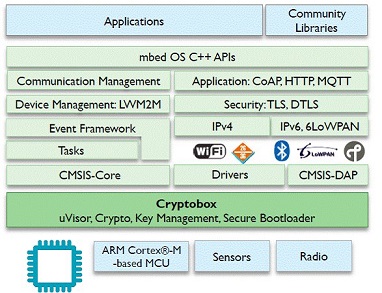
The arrow of design for connected cars will demand more development, bolstering the concept that software and embedded systems factored with newly-introduced actuators and sensors will become more prevalent. We’re talking about “software on wheels,” “SoC on wheels,” and “secured mobility.”

Design wise, the cost-effective trend will still remain with performance embedded systems. Many new cars may have extremely broad range of sensor and actuator‑based IoT designs which can be implemented on a single compact certified wireless module.

The arrow for connected cars will demand more development bolstering the concept that software and embedded systems factored with newly introduced actuators & sensors will become more prevalent; “software on wheels”, “SoC on wheels” and “secured mobility”.

Similarly, having fastest startup times by performing the task with a high-performance MCU vs MPU, is economic for a designer. It can not only reduce significant bill of materials cost, development resources, sculpted form factor, custom wireless design capabilities, but also minimize the board footprint. Aside from that, ARM has various IoT device development options, offering partner ecosystems with modules that have open standards. This ensures ease of IoT or connected car connectivity by having type approval certification through restrictive access to the communications stacks.

Drivers will be prompted with new end user applications — demand more deterministic code and processing with chips that support the secure memory capacity to build and house the software stack in these connected car applications.

Feature upon feature, layer upon layer of software combined with characteristics drawn from the events committed by drivers, tires, wheels, steering, location, telemetry, etc. Adapted speed and braking technologies are emerging now into various connected car makes, taking the traditional ABS concept to even higher levels combined with intelligence, along with controlled steering and better GPS systems, which will soon enable interim or cruise hands-free driving and parking.

Connected Car Evolution

Longer term, the technological advances behind the connected car will eventually lead to self-driving vehicles, but that very disruptive concept is still far out.

Where lies innovation and change is disruption

Like every eventual market disruption, there will be the in-between development of this connected car evolution. Innovative apps are everywhere, especially the paradigm where consumers have adopted to the seamless transitional experiences offered by apps and smartphones. Our need for ubiquitous connectivity and mobility, no matter where we are physically, is changing our vehicles into mobile platforms that want us users to seamlessly be connected to the world. This said demand for connectivity increases with the cost and devices involved will become more available. Cars as well as other mobility platforms are increasingly becoming connected packages with intelligent embedded systems. Cars are offering more than just entertainment — beyond providing richer multimedia features and in-car Internet access.  Further integration of secure and trusted vital data and connectivity points (hardware security/processing, crypto memory, and crypto authentication) can enable innovative navigation, safety and predictive maintenance capabilities.

Carmakers are worried about recent hacks,  especially with issues of security and reliability, making it unlikely that they will be open to every kind of app.  They’ll want to maintain some manufactured control framework and secure intrusion thwarting with developers, while also limiting the number of apps available in the car managing what goes or conflicts with the experience and safety measures.  Importantly, we are taking notice even now. Disruption comes fast, and Apple and others have been mentioned to enter this connected car market. This is the new frontier for technological equity scaling and technology brand appeal. Much like what we seen in the earlier models of Blackberry to smartphones, those late in the developmental evolution of their platforms may be forced adrift or implode by the market.

No one is arguing it will happen. Eventually, self-driving cars will arrive.  But for now, it remains a futuristic concept.

What can we do now in the invention, design and development process?

The broader output of manufactured cars will need to continue in leveraging new designs that take in more integration of traditional siloed integration vendors so that the emergence of more unified and centrally managed embedded controls can make its way. Hence, the importance now exists in the DNA of a holistically designed platform fitted with portfolio of processors and security to take on new service models and applications.

This year, we have compiled an interesting mixture of technical articles to support the development and engineering of car access systems, CAN and LIN networks, Ethernet in the car, capacitive interfaces and capacitive proximity measurement.

In parallel to the support of helping map toward the progress and evolution of the connected car, a new era of design exists. One in which the  platform demands embedded controls to evenly match their design characteristics and application use cases. We want to also highlight the highest performing ARM Cortex-M7 based MCU in the market, combining exceptional memory and connectivity options for leading design flexibility. The Atmel | SMART ARM Cortex-M7 family is ideal for automotive, IoT and industrial connectivity markets. These SAM V/E/S family of microcontrollers are the industry’s highest performing Cortex-M microcontrollers enhancing performance, while keeping cost and power consumption in check.

So are you designing for the latest automotive, IoT, or industrial product? Here’s a few things to keep in mind:

  • Optimized for real-time deterministic code execution and low latency peripheral data access
  • Six-stage dual-issue pipeline delivering 1500 CoreMarks at 300MHz
  • Automotive-qualified ARM Cortex-M7 MCUs with Audio Video Bridging (AVB) over Ethernet and Media LB peripheral support (only device in the market today)
  • M7 provides 32-bit floating point DSP capability as well as faster execution times with greater clock speed, floating point and twice the DSP power of the M4

We are taking the connected car design to the next performance level — having high-speed connectivity, high-density on-chip memory, and a solid ecosystem of design engineering tools. Recently, Atmel’s Timothy Grai added a unveiling point to the DSP story in Cortex-M7 processor fabric. True DSPs don’t do control and logical functions well; they generally lack the breadth of peripherals available on MCUs. “The attraction of the M7 is that it does both — DSP functions and control functions — hence it can be classified as a digital signal controller (DSC).” Grai quoted the example of Atmel’s SAM V70 and SAM V71 microcontrollers are used to connect end-nodes like infotainment audio amplifiers to the emerging Ethernet AVB network. In an audio amplifier, you receive a specific audio format that has to be converted, filtered, and modulated to match the requirement for each specific speaker in the car. Ethernet and DSP capabilities are required at the same time.

“The the audio amplifier in infotainment applications is a good example of DSC; a mix of MCU capabilities and peripherals plus DSP capability for audio processing. Most of the time, the main processor does not integrate Ethernet AVB, as the infotainment connectivity is based on Ethernet standard,” Grai said. “Large SoCs, which usually don’t have Ethernet interface, have slow start-up time and high power requirements. Atmel’s SAM V7x MCUs allow fast network start-up and facilitate power moding.”

Atmel has innovative memory technology in its DNA — critical to help fuel connected car and IoT product designers. It allows them to run the multiple communication stacks for applications using the same MCU without adding external memory. Avoiding external memories reduces the PCB footprint, lowers the BOM cost and eliminates the complexity of high-speed PCB design when pushing the performance to a maximum.

Importantly, the Atmel | SMART ARM Cortex-M7 family achieves a 1500 CoreMark Score, delivering superior connectivity options and unique memory architecture that can accommodate the said evolve of the eventual “SoC on wheels” design path for the connected car.

How to get started

  1. Download this white paper detailing how to run more complex algorithms at higher speeds.
  2. Check out the Atmel Automotive Compilation.
  3. Attend hands-on training onboard the Atmel Tech on Tour trailer. Following these sessions, you will walk away with the Atmel | SMART SAM V71 Xplained Ultra Evaluation Kit.
  4. Design the newest wave of embedded systems using SAM E70, SAM S70, or SAM V70 (ideal for automotive, IoT, smart gateways, industrial automation and drone applications, while the auto-grade SAM V70 and SAM V71 are ideal for telematics, audio amplifiers and advanced media connectivity).

IMG_3659

[Images: European Commission, GSMA]