
When you use solder paste to assemble your prototype PCB (printed circuit board) you need a stencil or hypodermic needle to apply the paste to the pads on the board. Then you use an IR (infra-red) reflow oven to melt the solder. Scott Fritz, an Atmel IC designer on the third floor, found this neat home-made controller that turns a cheap toaster oven into an IR reflow oven. I assume the name Reflowster is a combination of the words “reflow” and “toaster.”

The Reflowster will do closed-loop control of a cheap toaster over so you can do IR reflow soldering on your prototype circuit boards.
The Reflowster is an Arduino-based controller that that gives you predicable and repeatable heating and cooling profiles to melt the solder paste and connect up all the components on your board. They got their start on Kickstarter, and have actually shipped, so all the Kickstarter people are rewarded. Now the Reflowster folks are starting to offer the product to the general public.

The Reflow controller V3 PRO from PCB POOL in Europe is another product meant to work with a toaster oven.
I have mentioned a similar reflow controller made by the fine people at PCB-POOL in Europe. That article also described how my buddy Wayne Yamaguchi was using a toaster oven a decade ago to make his PCBs. Wayne did not use a controller. He just did a whole bunch of tests until he was satisfied he was getting good whetting and solder fillets on his circuit boards.
The great thing about the Reflowster is that it is a closed-loop controller. It is actually measures the temperature of the oven, and then controls the power to it so that the heating and cooling match the profiles recommended by component makers like Atmel (pdf).

Precise temperature control is needed to do quality lead-free soldering.
While I love, admire, and respect my buddy Wayne Yamaguch’s “theory of experiments” approach, you might really need the Reflowster. If you want to use different ovens, or have changing wall voltage, or the boards you are soldering are different sizes or have a different set of components on them, you want a closed-loop controller. If the chips have a big pad on the bottom, the die-attach-paddle, you need reflow. The other big factor is lead-free solder. Many of the crazy analog engineers I hang out with still use tin-lead solder for prototypes. It looks better, it feels better, and lead solder is more reliable. We also pull the solder off the reel by biting it gently and tugging, so we don’t have to set the soldering iron down. Lead poisoning might explain why we are all crazy. But if you are sane and insist on using lead-free solder, the preciseness of reflow control is important.

Solder paste application is like silkscreening T-shirts. Instead of silk the stencil is stainless steel. Instead of ink you use solder paste. Instead of T-shirts you do printed circuit boards.
Solder paste has its own hassles. You should refrigerate open containers so the little solder balls do not oxidize and change the reflow parameters. I am not sure the same caveat applies to when you use a big hypodermic to apply the solder paste. There the hassle is you have to do it one pad a time. A solder stencil is a thin stainless steel sheet where the PCB fab house has etched through all the areas where there is supposed to be solder. Sometimes called the “cream layer” Its not exactly the solder mask art, but it is pretty close, depending on your particular design. I know you can set up OrCAD 9.2 to do it, and I am sure other CAD packages can make it, or the PCB fab house can create one from your solder mask layer art.

Here is a typical solder stencil from Stencils Unlimited. With one swipe of a squeegee you apply solder paste to the pads for your chips and passive components.
The fine folks at Sunstone used to offer a free stencil, now it looks like they charge a little. Most fab houses can supply one. Assembly houses like Screaming Circuits or Advanced Assembly have the relationships with board houses to they can make your stencil when they assemble your boards. If you are really masochistic, and have a high-powered CO2 laser cutter handy, you can make your own stencils. You can also live in a cave and use flint tools, but I prefer to operate a little higher on the food chain. The LPKF laser mill can make your stencils as well.

This solder stencil from Proto-Advantage lets you apply solder paste for a QFN-32 chip.
There are also hybrid approaches. You can buy cheap solder stencils just for high-pin-count chips on your board. You squeegee the solder paste onto the board for each of those parts, Then you can use a hypodermic for the passive components or hand-solder them after you reflow the big chips.
If you are a big-time engineer on a big-budget project then just contact Screaming Circuits or Advanced Assembly or you local board assembly house (not PCB fab, but board assembly). I know Screaming Circuits can do it all since they have teamed up with Sunstone and Digi-Key. Just send Screaming Circuits the fab Gerber and fab files which they send to Sunstone, the assembly drawing and insert file which they use themselves, and the BOM (bill of material) they order the parts with from Digi-Key. They can do quick-turn and they can ship anywhere in the world.
So the prototyping ecosystem is like this:
- If you are a hobbyist use DIP (dual-inline plastic) chips with 0.1 inch lead spacing and through-hole passive components. You might use surface mount chips on DIP breakout boards.
- If you are a pro-hobbyist or low-budget engineer buy a temperature-controlled Weller soldering iron or a Metcal and a good stereo microscope. Now you can hand-solder surface mount boards. For chips with bottom pads you have to either heat the whole chip with a big soldering iron, use a heat gun, or try to wick the solder in from vias you design in on the backside of the board.
- If you are a hobbyist doing low-volume manufacturing or a medium-budget engineer, go to solder stencils and reflow ovens.
- If you are a hobbyist that hit it big or a big-budget engineer, use the board house to order the parts, get the PCB fab, and assemble and maybe even test your board.

TQM Solutions knows that total quality management means you not only have a mountain of documentation, but that you organize that mountain.
Note that last item. See, as an engineer, your real job is to make a set of documentation so the design can get manufactured by non-engineers and non-technicians and non-hobbyists. Its nice you are a hands-on person. Heck, its critical you are a hands-on person to be a good engineer. But your real responsibility is making sure the CAD files are correct. it might speed things up if you make a first-spin board yourself, and its neat if you make the board on an LPKF mill and you can get parts from the factory floor or Radio Shack or a salvage yard.

I used to design products with parts I found cheap at places like Weird Stuff Warehouse in Silicon Valley. Then one of my designs went to production but Weird Stuff had sold off all the parts I had used. Now I select parts from distributors.
The great thing about using Screaming Circuits and Sunstone and a distributor like Mouser or Arrow or Newark or DigiKey is that you are proving out your documentation. You make it clear to Screaming Circuits that if your pick-and-place insert file has mistakes they tell you, you fix them and they use that file. This way, when they see that the part origin for a DPAK is at the pad and not the part center, they know the vacuum picker cannot pick it up, so you catch that AND FIX IT. If your Gerbers have problems you make sure Sunstone tells you, or you use the free DFM (Design for manufacturing) check offered by Advanced Circuits. Then you FIX THE FILES. Same deal for any BOM mistakes. Make sure somebody tells you so you can FIX THE FILE, and not the text file, you fix the CAD file in OrCAD or Altium or whatever, so it spits out a perfect BOM.
Now when you send the CAD files to China to get assembled on the cheap, you know the files are correct. Anything less and you are not an engineer, you are an amateur. Proto Express even works with a Chinese partner to ensure you can get cheap-high volume boards that work as well at the Proto-Express boards made right here in Silicon Valley.
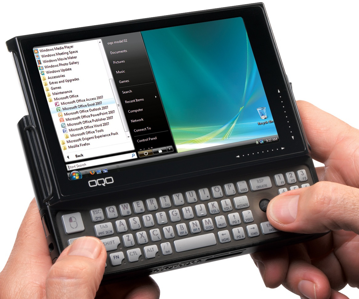
The oqo Model 2 used a Via processor. The third model with an Intel Atom never got built since they ran out of money (courtesy Engadget).
This level of diligence and exactness is critical. I worked at oqo, a San Francisco start-up that made the first palm-top computer that ran real Windows OS. The first model was based on the Transmeta “emulated” x86 processor. The second model used a Via chip. Lesson there is never base a business plan on being smarter than Intel. The third prototype never went into production. I had left the company for National Semiconductor, but pals there told me they used an Intel Atom processor and it was a real product that could really work good. But they were running out of money. So I assume in a big rush, they sent the design to the Chinese contract manufacturer. A pal familiar with the company told me oqo had to fly out an engineer to China and there were 1000 ECOs (engineering change orders) to get the design ready for high-volume manufacturing. One thousand mistakes. Now it probably didn’t matter, but its nice to think that if they had scrubbed the CAD files, the fab, the assembly, and the rework documentation through a US quick-turn prototype manufacturer, and fixed most of those mistakes, then maybe they could have gotten that product to market and saved the company.
This is a perfect example of the asymmetric respect problem in engineering. The Chinese manufacturing engineers respected those high-tone former Apple designers at oqo. But the oqo engineers may have thought manufacturing was some triviality and beneath them. Perhaps they thought any idiot should be able to do it. Sorry. Wrong. Dead wrong. Dead just like oqo is today. You need to be every bit as smart, clever, and creative to do manufacturing and test as to do design work. When you take a product all the way to production, you will learn to respect everybody involved. Respect the planners, the clerks, the assemblers, and ALL the engineers. So be a good and respectful design engineer and make sure your CAD files are a good as they can be before you send them out for production. That is your responsibility, not a Flextronics responsibility.
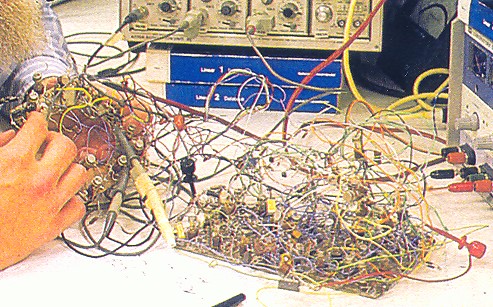
The cover of my mentor Bob Pease’s book Troubleshooting Analog Circuits has one of his “airball” prototypes on the cover. Application engineers like Bob can do proof-of-concept, but don’t try sending this out for high-volume manufacturing.
So like all things, prototyping has an analog continuum to it, There is a place for quick-and dirty hacks. There is place for super-diligence. And there is a whole spectrum of tradeoffs for an appropriate design effort in between those poles. Just don’t do some rush-job today that you just know will bite you a few months later.
[Update] I showed this post to Wayne Yamaguchi and he had this great comment:
“One of the major drawbacks to solder paste is the shelf life. No matter how you buy it, the container and contents will go bad in about 6 months time, even in the refrigerator. It’s the flux that ages and slowly solidifies making the reflow consistency different over time. It’s just a real pain to dispense the paste with a tiny-tip syringe when it it’s fresh, and even worse when it has aged a bit. If I recall correctly, the smallest syringe runs about $50.00. You can solder a lot with that but if you only make one proto this is an expensive proposition.
“Mine tends to absorb water over time and this makes it pop when reflowing, blowing off chunks of solderpaste in all directions. I can hand-solder 0402 and DFN parts with the soldering iron. I only need the hot-air station for pads that are not exposed, like power pads and some SMT inductors. I would recommend a really good soldering iron or two, and a general-purpose hot air station if you want to hand-solder small runs of boards. You will need one with a 0.2mm tip or smaller for the leadless and 0402 parts.
“I prefer to still use leaded solder. It solders at a lower temp and the chemicals are less caustic, unlike the solder flux used for leadless solder. Unless I have to, I try to use “no clean” flux and occasionally will use Kester 331 (IIRC) for gold-plated pads.
“Good stencils are cut non-vertical. The edges are beveled so the bottomside is slightly larger than the top, making the solderpaste less resistant to sticking to the stencil. Hopefully, when you lift the stencil the solderpaste adheres to the PCB and not the stencil. I’ve never actually seen the process, but, I always imagined that the paste would not all tranfer. I guess it works. Just doesn’t work in my mind. The bevel is only 5-10 degrees. Hardly noticeable by the eye, but, I guess it makes a difference.
“Another gotcha will come when you doing rework. You remove the part in question and/or use solderwick to clean the pads. If you try and apply solderpaste right away the residual heat will outflow the flux from the syringe tip which is most frustrating as now the tip is full of paste with no flux. When this occurs it is like concrete and won’t flow. It is possible to drain more than the tip into the larger part of the syringe tube rendering the whole syringe load bad. You can unscrew the tip and plunge out the bad material, but, who knows if you now have the right ratio of flux to solder anymore? If this is the tube from the vendor you can kiss $50.00 down the drain. If you transferred solderpaste to a smaller syringe the loss is less than $50.00.”
I guess all those years at HP and Agilent, and then being in business for himself gave Wayne a valuable perspective on prototyping. Many thanks to him, and add you own comments below.

Hi,
I was looking for some information on PCB Assembly today when I came across your excellent article:
Great stuff!
Actually, I just put together an infographic about “PCB Reliability: Via Design” and “Regulatory Testing and Certifications”. As someone that likes to write about PCB Assembly and Design, I thought you might get a kick out of it.
Let me know if you want to check it out.
Cheers,
Algen
LikeLike
Sure, please send me your email and we would like to see it.
LikeLike