Tag Archives: China

IR reflow oven for your prototype PCBs

When you use solder paste to assemble your prototype PCB (printed circuit board) you need a stencil or hypodermic needle to apply the paste to the pads on the board. Then you use an IR (infra-red) reflow oven to melt the solder. Scott Fritz, an Atmel IC designer on the third floor, found this neat home-made controller that turns a cheap toaster oven into an IR reflow oven. I assume the name Reflowster is a combination of the words “reflow” and “toaster.”
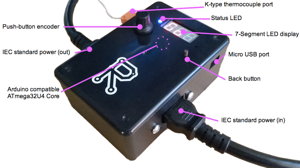
annotated_reflowster

The Reflowster will do closed-loop control of a cheap toaster over so you can do IR reflow soldering on your prototype circuit boards.

The Reflowster is an Arduino-based controller that that gives you predicable and repeatable heating and cooling profiles to melt the solder paste and connect up all the components on your board. They got their start on Kickstarter, and have actually shipped, so all the Kickstarter people are rewarded. Now the Reflowster folks are starting to offer the product to the general public.
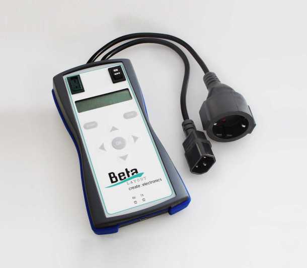
PCB-POOL_IR-reflow-controller

The Reflow controller V3 PRO from PCB POOL in Europe is another product meant to work with a toaster oven.

I have mentioned a similar reflow controller made by the fine people at PCB-POOL in Europe. That article also described how my buddy Wayne Yamaguchi was using a toaster oven a decade ago to make his PCBs. Wayne did not use a controller. He just did a whole bunch of tests until he was satisfied he was getting good whetting and solder fillets on his circuit boards.

The great thing about the Reflowster is that it is a closed-loop controller. It is actually measures the temperature of the oven, and then controls the power to it so that the heating and cooling match the profiles recommended by component makers like Atmel (pdf).

Atmel-IR-reflow-profile

Precise temperature control is needed to do quality lead-free soldering.

While I love, admire, and respect my buddy Wayne Yamaguch’s “theory of experiments” approach, you might really need the Reflowster. If you want to use different ovens, or have changing wall voltage, or the boards you are soldering are different sizes or have a different set of components on them, you want a closed-loop controller. If the chips have a big pad on the bottom, the die-attach-paddle, you need reflow. The other big factor is lead-free solder. Many of the crazy analog engineers I hang out with still use tin-lead solder for prototypes. It looks better, it feels better, and lead solder is more reliable. We also pull the solder off the reel by biting it gently and tugging, so we don’t have to set the soldering iron down. Lead poisoning might explain why we are all crazy. But if you are sane and insist on using lead-free solder, the preciseness of reflow control is important.
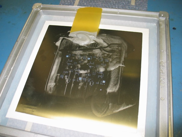
Solder-stencil-squeegee-Wintech-Electronics

Solder paste application is like silkscreening T-shirts. Instead of silk the stencil is stainless steel. Instead of ink you use solder paste. Instead of T-shirts you do printed circuit boards.

Solder paste has its own hassles. You should refrigerate open containers so the little solder balls do not oxidize and change the reflow parameters. I am not sure the same caveat applies to when you use a big hypodermic to apply the solder paste. There the hassle is you have to do it one pad a time. A solder stencil is a thin stainless steel sheet where the PCB fab house has etched through all the areas where there is supposed to be solder. Sometimes called the “cream layer” Its not exactly the solder mask art, but it is pretty close, depending on your particular design. I know you can set up OrCAD 9.2 to do it, and I am sure other CAD packages can make it, or the PCB fab house can create one from your solder mask layer art.

Solder-stencil_PCB-stencilsunlimited

Here is a typical solder stencil from Stencils Unlimited. With one swipe of a squeegee you apply solder paste to the pads for your chips and passive components.

The fine folks at Sunstone used to offer a free stencil, now it looks like they charge a little. Most fab houses can supply one. Assembly houses like Screaming Circuits or Advanced Assembly have the relationships with board houses to they can make your stencil when they assemble your boards. If you are really masochistic, and have a high-powered CO2 laser cutter handy, you can make your own stencils. You can also live in a cave and use flint tools, but I prefer to operate a little higher on the food chain. The LPKF laser mill can make your stencils as well.

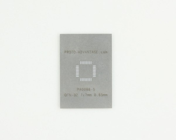
Solder-stencil_QFN-32_Proto-Advantage

This solder stencil from Proto-Advantage lets you apply solder paste for a QFN-32 chip.

There are also hybrid approaches. You can buy cheap solder stencils just for high-pin-count chips on your board. You squeegee the solder paste onto the board for each of those parts, Then you can use a hypodermic for the passive components or hand-solder them after you reflow the big chips.

If you are a big-time engineer on a big-budget project then just contact Screaming Circuits or Advanced Assembly or you local board assembly house (not PCB fab, but board assembly). I know Screaming Circuits can do it all since they have teamed up with Sunstone and Digi-Key. Just send Screaming Circuits the fab Gerber and fab files which they send to Sunstone, the assembly drawing and insert file which they use themselves, and the BOM (bill of material) they order the parts with from Digi-Key. They can do quick-turn and they can ship anywhere in the world.

So the prototyping ecosystem is like this:

  • If you are a hobbyist use DIP (dual-inline plastic) chips with 0.1 inch lead spacing and through-hole passive components. You might use surface mount chips on DIP breakout boards.
  • If you are a pro-hobbyist or low-budget engineer buy a temperature-controlled Weller soldering iron or a Metcal and a good stereo microscope. Now you can hand-solder surface mount boards. For chips with bottom pads you have to either heat the whole chip with a big soldering iron, use a heat gun, or try to wick the solder in from vias you design in on the backside of the board.
  • If you are a hobbyist doing low-volume manufacturing or a medium-budget engineer, go to solder stencils and reflow ovens.
  • If you are a hobbyist that hit it big or a big-budget engineer, use the board house to order the parts, get the PCB fab, and assemble and maybe even test your board.
TQM Solutions knows that total quailty managemnt means you not only have a mountain of documentation, but that you organize that mountain.

TQM Solutions knows that total quality management means you not only have a mountain of documentation, but that you organize that mountain.

Note that last item. See, as an engineer, your real job is to make a set of documentation so the design can get manufactured by non-engineers and non-technicians and non-hobbyists. Its nice you are a hands-on person. Heck, its critical you are a hands-on person to be a good engineer. But your real responsibility is making sure the CAD files are correct. it might speed things up if you make a first-spin board yourself, and its neat if you make the board on an LPKF mill and you can get parts from the factory floor or Radio Shack or a salvage yard.

Salvage-yard-electronics-Weird-Stuff-Warehouse

I used to design products with parts I found cheap at places like Weird Stuff Warehouse in Silicon Valley. Then one of my designs went to production but Weird Stuff had sold off all the parts I had used. Now I select parts from distributors.

The great thing about using Screaming Circuits and Sunstone and a distributor like Mouser or Arrow or Newark or DigiKey is that you are proving out your documentation. You make it clear to Screaming Circuits that if your pick-and-place insert file has mistakes they tell you, you fix them and they use that file. This way, when they see that the part origin for a DPAK is at the pad and not the part center, they know the vacuum picker cannot pick it up, so you catch that AND FIX IT. If your Gerbers have problems you make sure Sunstone tells you, or you use the free DFM (Design for manufacturing) check offered by Advanced Circuits. Then you FIX THE FILES. Same deal for any BOM mistakes. Make sure somebody tells you so you can FIX THE FILE, and not the text file, you fix the CAD file in OrCAD or Altium or whatever, so it spits out a perfect BOM.

Now when you send the CAD files to China to get assembled on the cheap, you know the files are correct. Anything less and you are not an engineer, you are an amateur. Proto Express even works with a Chinese partner to ensure you can get cheap-high volume boards that work as well at the Proto-Express boards made right here in Silicon Valley.
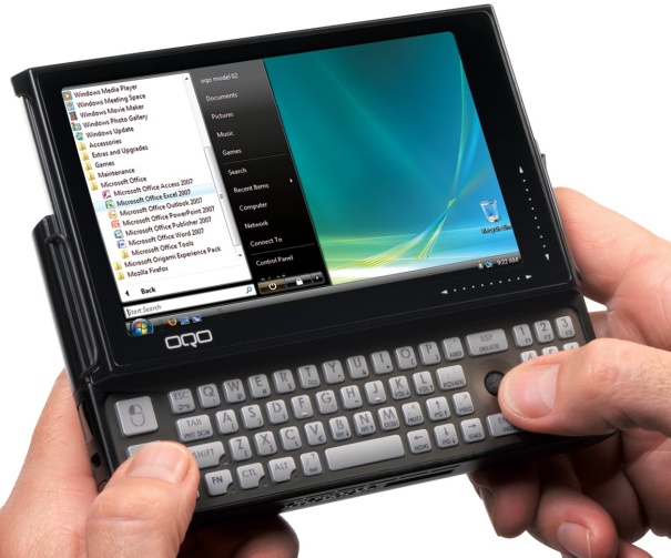
oqo-model-02_Engadget

The oqo Model 2 used a Via processor. The third model with an Intel Atom never got built since they ran out of money (courtesy Engadget).

This level of diligence and exactness is critical. I worked at oqo, a San Francisco start-up that made the first palm-top computer that ran real Windows OS. The first model was based on the Transmeta “emulated” x86 processor. The second model used a Via chip. Lesson there is never base a business plan on being smarter than Intel. The third prototype never went into production. I had left the company for National Semiconductor, but pals there told me they used an Intel Atom processor and it was a real product that could really work good. But they were running out of money. So I assume in a big rush, they sent the design to the Chinese contract manufacturer. A pal familiar with the company told me oqo had to fly out an engineer to China and there were 1000 ECOs (engineering change orders) to get the design ready for high-volume manufacturing. One thousand mistakes. Now it probably didn’t matter, but its nice to think that if they had scrubbed the CAD files, the fab, the assembly, and the rework documentation through a US quick-turn prototype manufacturer, and fixed most of those mistakes, then maybe they could have gotten that product to market and saved the company.

This is a perfect example of the asymmetric respect problem in engineering. The Chinese manufacturing engineers respected those high-tone former Apple designers at oqo. But the oqo engineers may have thought manufacturing was some triviality and beneath them. Perhaps they thought any idiot should be able to do it. Sorry. Wrong. Dead wrong. Dead just like oqo is today. You need to be every bit as smart, clever, and creative to do manufacturing and test as to do design work. When you take a product all the way to production, you will learn to respect everybody involved. Respect the planners, the clerks, the assemblers, and ALL the engineers. So be a good and respectful design engineer and make sure your CAD files are a good as they can be before you send them out for production. That is your responsibility, not a Flextronics responsibility.
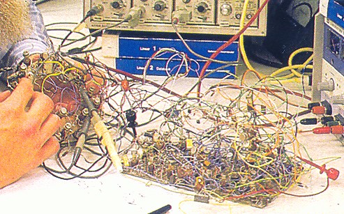
Bob-Pease-air-ball-prototype

The cover of my mentor Bob Pease’s book Troubleshooting Analog Circuits has one of his “airball” prototypes on the cover. Application engineers like Bob can do proof-of-concept, but don’t try sending this out for high-volume manufacturing.

So like all things, prototyping has an analog continuum to it, There is a place for quick-and dirty hacks. There is place for super-diligence. And there is a whole spectrum of tradeoffs for an appropriate design effort in between those poles. Just don’t do some rush-job today that you just know will bite you a few months later.

[Update] I showed this post to Wayne Yamaguchi and he had this great comment:

“One of the major drawbacks to solder paste is the shelf life.  No matter how you buy it, the container and contents will go bad in about 6 months time, even in the refrigerator.  It’s the flux that ages and slowly solidifies making the reflow consistency different over time.  It’s just a real pain to dispense the paste with a tiny-tip syringe when it it’s fresh, and even worse when it has aged a bit. If I recall correctly, the smallest syringe runs about $50.00.  You can solder a lot with that but if you only make one proto this is an expensive proposition.

“Mine tends to absorb water over time and this makes it pop when reflowing, blowing off chunks of solderpaste in all directions. I can hand-solder 0402 and DFN parts with the soldering iron.  I only need the hot-air station for pads that are not exposed, like power pads and some SMT inductors. I would recommend a really good soldering iron or two, and a general-purpose hot air station if you want to hand-solder small runs of boards. You will need one with a 0.2mm tip or smaller for the leadless and 0402 parts.

“I prefer to still use leaded solder.  It solders at a lower temp and the chemicals are less caustic, unlike the solder flux used for leadless solder.  Unless I have to, I try to use “no clean” flux and occasionally will use Kester 331 (IIRC) for gold-plated pads.

“Good stencils are cut non-vertical.  The edges are beveled so the bottomside is slightly larger than the top, making the solderpaste less resistant to sticking to the stencil.  Hopefully, when you lift the stencil the solderpaste adheres to the PCB and not the stencil.  I’ve never actually seen the process, but, I always imagined  that the paste would not all tranfer.  I guess it works.  Just doesn’t work in my mind.  The bevel is only 5-10 degrees.  Hardly noticeable by the eye, but, I guess it makes a difference.

“Another gotcha will come when you doing rework.  You remove the part in question and/or use solderwick to clean the pads.  If you try and apply solderpaste right away the residual heat will outflow the flux from the syringe tip which is most frustrating as now the tip is full of paste with no flux.  When this occurs it is like concrete and won’t flow.  It is possible to drain more than the tip into the larger part of the syringe tube rendering the whole syringe load bad.  You can unscrew the tip and plunge out the bad material, but, who knows if you now have the right ratio of flux to solder anymore?  If this is the tube from the vendor you can kiss $50.00 down the drain.  If you transferred solderpaste to a smaller syringe the loss is less than $50.00.”

I guess all those years at HP and Agilent, and then being in business for himself gave Wayne a valuable perspective on prototyping. Many thanks to him, and add you own comments below.

3D printing wrist splints

Loughborough University lecturer Dr. Abby Paterson has developed an innovative app that will allow clinicians to easily design and manufacture a new generation of custom-made 3D printed wrist splints.

According to 3DERS, the next-gen splints are more comfortable, attractive and affordable than current options.

“I wanted to give clinicians the ability to make splints that they have not been able to make before,” said Paterson. “They can improve the aesthetics, the fit, and integrate extra bits of functionality they couldn’t do before.”

As Paterson notes, the splints, which provide joint protection, rest, and promote pain relief, could be a major boost for sufferers of rheumatoid arthritis.

Dr. Bibb, who supervised Paterson’s PhD, said he believes the new splints will be cost-effective.

“We are in the development phase. The research has proved that this is desirable and the clinicians want it. We know there’s lots of potential.”

As we’ve previously discussed on Bits & Pieces, 3D printing technology – projected to be a $3 billion business by 2016 – is rapidly evolving, particularly in the medical space. Indeed, 3D printed orthopedic implants were recently fitted in Peking’s University Third Hospital in Beijing, while doctors at the Kyoto University Graduate School of Medicine in Japan successfully transplanted 3D printed bones into four patients with cervical spine (cervical) disc herniation.

Similarly, 3D printing tech helped doctors at the First Affiliated Hospital of Xi’an Jiaotong University repair a patient’s damaged skull in China, while researchers at the Huazhong University of Science and Technology used 3D printing technology to create living human kidneys. In September, scientists at Nottingham Trent University and Nottingham University Hospitals NHS (UK) Trust announced the development of an electronic smart pump to help victims of chronic heart failure.

Of course, the DIY Maker Movement has been using Atmel-powered 3D printers like MakerBot and RepRap for some time now. However, 3D printing has clearly entered a new and important stage in a number of spaces including the medical spherearchitectural arenascience lab and even on the battlefield.

Businessweek says Makers are gaining ground in China

Writing for Bloomberg Businessweek, Christina Larson confirms that the Maker Movement continues to gain significant ground in China.

Indeed, the popularity of XinCheJian, which means “new factory,” is a sign of China’s continued participation in the global Maker Movement, which former Wired editor Chris Anderson describes as a “third industrial revolution” characterized by open-source design, 3D printing, and crowdfunding.

As Larson notes, 30 independent hackerspaces, including XinCheJian, have already opened across the country.

“DIY culture may be a little slower to pick up in China, but we’re closer to the supply chain,” David Li, a Taiwan-born programmer who co-founded XinCheJian in 2011, told the publication.

“Everyone knows someone who works in manufacturing. That makes it easier to move ideas from hobbyist tinkering to larger production runs. Makers turn startup much faster in China. That’s why governments in Shanghai and other cities, eager to jump-start innovation, are supporting the movement.”

To be sure, the Shanghai government initiated a program in 2011 to create 100 hackerspaces in the city, offering each up to 500,000 yuan ($80,000) in funding.

Shenzhen (Image Credit: Wikipedia)

In 2012, XinCheJian and DFRobot co-sponsored a Shanghai maker carnival with the Communist Youth League.

Unsurprisingly, the Maker Movement has captured the attention of numerous Chinese industry leaders, including Foxconn and PCH International, two co-sponsors of Maker Faire Shenzhen.

Interested in learning more? The full text of “The Maker Movement Gains Ground in China” can be read here on Businessweek. Readers may also want to check out our Bits & Pieces article archive on the subject here.

What’s inside Xiaomi’s MiPad?

The China-based IT168 crew recently published a detailed teardown of Xiaomi’s MiPad that was translated by the folks at GizmoChina.

The popular Android tablet – which hit the streets back in May – features Nvidia’s quad-core 2.2GHz Tegra K1 processor, a 7.9-inch 2048 x 1536 display, Atmel’s MXT1664T touchscreen chip, 2GB RAM, 16/64GB of memory, Wifi, 6700mAh battery and a 5mP/8mP Sony dual-camera.

As the IT168 crew notes, the MiPad is made of very sturdy materials, with the tablet’s interior boasting a three-section design covered with plastic for stability and cooling.

“The MiPad uses the most up-to-date chips around including the BCM4354 and Atmel’s T touchscreen chips,” writes Frank Tu of GizmoChina.

“It is also the first appearance of the Tegra K1. The MiPad is probably the most powerful tablet around when it comes to performance.”

Interested in learning more? You can read about Xiaomi’s MiPad on AnandTech here.

Qiyang’s QY-A5D3XEK is a SAMA5D3 dev board


Based in Hangzhou, China, Qiyang Technology (杭州启扬智能科技有限公司) is a company that specializes in embedded hardware solutions such as the QY-A5D3EK development board which was recently featured on CNX-Software.

The platform comprises a base board (IAC-A5D3X-MB) and computer-on-module (ICA-A5D3X_CM) equipped with the following specs:

  • 

Atmel SAMA5D3 ARM Cortex A5 @ 536 MHz
  • 256 MB DDR2 @ 333 MHz
  • 
256MB NAND flash + 2MB dataflash on CoM, 2x SD card slot on baseboard
  • VGA and 16-bit TFT LCD (24-bit compatible) interface up to 2048×2048
  • 
AC97 codec, 1x mic input, 1x LINE in, 1x LINE out
  • 10/100M Ethernet
  • 5x RS232 ports including one as a debug port (DB9), 2x RS232/RS485 ports
  • 1x USB 2.0 host ports, 1x micro USB OTG port
  • Headers – GPIO, PWM, SPI, I2C, JTAG, EBI CAN bus, 8×8 keyboard matrix header (also used as 4-wire resistive touchscreen I/F)
  • Wake-up and reset buttons
  • +12V power supply, supports +6V to 23V input
  • -20 to 70 C (operating) temperature range

“The company provides support for Linux 3.6.9 + Qt4, as well as Android 4.0 for the board which are provided with the documentation and tools on a DVD,” a CNX-Software writer noted.

“[Plus], Qiyang offers various LCD panels compatible with their board from 4.3″ to 10.4″, as well as optional TTL to LVDS or TTL to VGA modules.”

The IAC-A5D3X-KIT is currently available, with a sample price of $180 per unit.

Interested in learning more? You can check out the product’s official page here.

Report: China invests heavily in Makers


China’s Communist Party government has reportedly endorsed the country’s burgeoning DIY Maker Movement.

“Innovation is no longer only promoted by the top-down initiatives of the world’s biggest companies,” reads a recent article in the state-run Liberation Daily newspaper.

“[Rather, it] is being built from the bottom up by countless individuals such as amateurs, entrepreneurs and professionals. As [Chris] Anderson says, we are born Makers… The future of China’s maker industry will be very competitive.”

Another state media article expresses similar sentiments, recommending that authorities “seize the current opportunity to introduce plans as soon as possible to support the development of the maker movement.”

As Emily Parker notes in Slate, both the United States and China are embracing the Maker Movement’s potential for entrepreneurship, viewing this kind of grass-roots innovation as essential for staying competitive in the 21st -century economy.

“The 2012 Shanghai Maker Carnival had the support of the Communist Youth League. Shanghai officials proposed 100 government-supported ‘innovation houses.’ Beijing’s Tsinghua University embraces Maker-inspired education,” she writes.

“Some hackerspaces in China get official support in the form of equipment, or help with paying the rent.”

Eric Pan, the Sichuan-born founder of Seeed Studio, explains why.

“Innovation can lead to start-ups. Start-ups can solve the problems of unemployment, and start-ups also have potential to become technology and design-intensive companies.”

Indeed, as Pan told Bits & Pieces earlier this year, MakerSpaces will likely enable a new wave of tech startups in China as in the US.

“To be sure, Makers working with their peers are now able to more easily realize their goals, while bringing products to market with new platforms such as e-commerce sites and crowd funding… For now, MakerSpaces are gradually helping Chinese tech companies discover additional possibilities, although the Maker role is likely to increase, with participants in the DIY culture setting technology trends in conjunction with major industries,” he adds.

The full text of Emily Parker’s “The Chinese Government Is Investing Heavily in the Maker Movement” is available on Slate here.

Atmel looks back at Maker Faire Shenzhen

Dale Dougherty, founder of MAKE Magazine and creator of Maker Faire, notes that Maker Faire Shenzhen, held the first weekend of April 2014, celebrated the emergence of the Maker Movement in China and recognized the significance of Shenzhen as a global capital for DIY culture.

“Maker Faire Shenzhen was the first full-scale Maker Faire in China. An estimated 30,000 people walked the tree-lined streets to interact with makers, participate in workshops and listen to presentations,” Dougherty explained in a recent Makezine article.

“[The event] was a showcase for 300 makers who manned 120 exhibits. Organized by Eric Pan and his team at Seeed Studio, Maker Faire Shenzhen was a public demonstration of the robust productivity of China’s makers. The Maker Movement could play a major role in China in transforming both China’s view of itself and the world’s view of China as a center of innovation.”

As we’ve previously discussed on Bits & Pieces, Atmel attended the Faire from April 6-7. Our booth – #4 – was located right next to Center Stage.

In addition, Sander Arts (@Sander1Arts), VP of Corporate Marketing at Atmel, gave a detailed presentation about Atmel microcontrollers, the IoT and Makers.

Sander’s well-attended presentation garnered a significant amount of attention in the local press from a number of journalists, including those writing for CNET, Ifanr, LeiPhone, PowerSystemsDesign (China) and 01EA.

“Various Maker teams demonstrated their projects, ranging from 3D printers to open-source vehicles, VR and wearable devices at Maker Faire 2014 in Shenzhen, highlighting the extensive possibilities of the Internet of Things,” wrote Cui Qiwen, Ifanr.com.

“As the robust brain behind all these maker projects, Atmel was also present at the convention.”

Xia Hang of LeiPhone, expressed similar sentiments.

“… Atmel accounts [for a] significant role that drives and inspires various projects in different categories such as LED, 3D printing and Arduino. Atmel’s MCU-based Arduino development platform enables more entry-level [projects],” Hang explained.

“Through Maker communities, Atmel has constructed close relationships with Makers in mainland China, not only by providing technology support, but also offering opportunities to present their maker projects through holding AVR Hero Contests. [As Sander says], ‘we are the Makers’ enablers, but the power is with you.'”

Meanwhile, CNET’s Tao Jingjie confirmed that Atmel maintains a close relationship with Makers via its AVR-based 8-bit MCUs and ARM-based 32-bit MCUs/MPUs.

“Atmel powers Makers to convert innovative ideas into actually commercialization-possible products, including LED projects, 3D printing projects, Arduino projects, and so on,” said Jingjie.

“It also held the global AVR Hero design contest, in which the products [that won] the award will achieve funding from Atmel [along with help] to enter the market in the future.”

Interested in learning more about the Maker Movement in China? You can check out our article archive on the subject here.

Makers tap into China’s open hardware scene

Writing for CNBC, Lynn Lee notes that a grassroots innovation movement centered around open hardware and Maker culture is evolving in China.

“Where high-tech research and development was once seen as something only large companies could afford, more and more individuals are going it on their own,” Lee explained.

Image Credit: CNET China

To be sure, hackerspaces, which Lee describes as “key” to a booming DIY or Maker Movement, were non-existent in the China of 2010. However, the global concept has quickly taken off in a number of Chinese cities such as Shenzhen, Shanghai and Beijing.

“There are people here who are passionate about the maker culture and innovation. There is an open hardware scene in China tapped into the global maker movement and it is growing,” Dr. Silvia Lindtner of the University of California, Irvine and Fudan University in Shanghai told CNBC.

Image Credit: CNET China

“In recent years, China has become an essential enabler in the global maker movement. That’s because many factories in Shenzhen have long adopted a system of open-source sharing in order to lower production costs.”

Lee also highlighted the Shenzhen-based Seeed Studio founded by Eric Pan, which works to combine the potential of open-source hardware with opportunities offered by Guangdong’s electronics supply chain.

“Makers looking to produce prototypes of their designs and small batches of samples can turn to Seeed for help,” Lee noted. “The company also hosts an active community on its site, where proposals are pitched and projects with the most support are manufactured and made available for sale.”

As we’ve previously discussed on Bits & Pieces, Eric is understandably enthusiastic about the open source movement, as he also organized the Shenzhen Maker Faire and established the hardware incubation project “HAXLR8R” with Cyril Ebersweiler.

“MakerSpaces will likely enable a new wave of tech startups in China as in the US. To be sure, Makers working with their peers are now able to more easily realize their goals, while bringing products to market with new platforms such as e-commerce sites and crowdfunding,” Pan told Bits & Pieces during a recent interview.

Shenzhen (Image Credit: Wikipedia)

“MakerSpaces are gradually helping Chinese tech companies discover additional possibilities, although the Maker role is likely to increase, with participants in the DIY culture setting technology trends in conjunction with major industries.”

Interested in learning more about China and the Maker Movement? You can check out our article archive on the subject here.

From Shanzhai to OSHW: The Maker Movement in China

Although the Maker and open source hardware movements are a global phenomenon, the DIY culture in China can actually be traced back to the ancient concept of Shanzhai. As Gabrielle Levine, the newly appointed president of the Open Source Hardware Association (OSHWA) notes, China is going to be a huge driving force in the open source hardware landscape.

“There are many similarities between [the local concept of] Shanzhai and the open source hardware community,” Gabriella Levine told OpenElectronics in February. “Both Shanzhai and open source hardware projects borrow information, tools, source code, CAD files and techniques; both improve upon other’s work to accelerate development.”

SeeedStudio founder Eric Pan expressed similar sentiments during a recent interview with Atmel’s official blog, Bits & Pieces.

“MakerSpaces will likely enable a new wave of tech startups in China as in the US,” he confirmed.

“Clearly, hardware development is becoming a more agile process with the aid of [open source] prototyping tools like RepRap and Arduino boards – both of which are helping to facilitate innovation across the world and particularly in China.”

Similarly, David Li, co-founder of Shanghai’s first Maker Space, told The Economist that the DIY movement has inspired the creation of legitimate and innovative products, with socially progressive Makers teaming up with more traditional manufacturers in China.

We at Atmel are at the strategic heart of the international Maker Movement, with a comprehensive portfolio of versatile microcontrollers (MCUs) that power a wide range of Maker platforms and devices, including 3D printers (MakerBot Replicator 2 and RepRap), the vast majority of Arduino boards, as well as Adafruit’s Gemma, Trinket and Flora platforms.

Indeed, Arduino boards are currently used by millions of Makers, engineers, schools and corporations all over the world. At least 1.2 million Atmel-powered Arduino boards have been sold to date, with the ATmega328-based Uno being a particular Maker and prototyping favorite. Of course, stand-alone AVR microcontrollers like the tinyAVR lineup are also popular amongst the DIY crowd.

As we’ve previously discussed on Bits & Pieces, an increasing number of Makers are kicking off project prototyping with Atmel-based Arduino boards. Concurrently, we are also seeing a jump in professional engineers relying on Atmel-powered Arduino boards to create initial models for their devices, platforms and solutions.

According to Gartner, 50% of companies expected to help build the rapidly evolving Internet of Things have yet to coalesce. This is precisely why Atmel views China’s Maker Movement as one of the primary tech incubators for future IoT companies and devices, many of which will undoubtedly use Atmel microcontrollers (MCUs) to power their respective platforms.

Atmel will proudly be attending Maker Faire Shenzhen this year on April 6-7. Our booth – #4 – is located right next to Center Stage. We’ll be showcasing a number of Atmel-powered products including a Zigebee-based lighting demo, robotic model car, various Seeeduino boards, the Rainbow Cube (LED light controlled by Atmel MCUs) and an e-ink badge.

I’ll also be giving a presentation about Atmel microcontrollers, the IoT and Makers at 2PM on April 7th at the Center Stage. Hope to see you there!

Will Makers change Shenzhen?

Writing for the EE Times, Junko Yoshida says local culture in Shenzhen is rapidly changing, with a growing number of hi-tech workers reportedly joining the rapidly growing Maker Movement (chuang ke).

Indeed, RPTechWorks founder Yang Yango told Yoshida that “labor intensive” Shenzhen will eventually become a city known for fast prototyping with “shortened development” cycles. 

Qifeng Yan, ex-director of the Nokia Research Center in Shenzhen and currently director and chief researcher at Media Lab (Shenzhen) of Hunan University, expressed similar sentiments in an interview with Yoshida.

However, Yan noted that many individuals in Shenzhen lack free time and space. As such, the Maker Movement in Shenzhen (and China as a whole) is evolving into something quite distinct. 

More specifically, it is intertwined with the existing electronics ecosystem in Shenzhen, as Makers help local companies open DIY workshops, kick off fresh projects and even open new startups.

“The electronics market on Huanqiang Road has always been a destination for every EE. But its importance is increasing for the rest of us, with the maker movement catching on,” Yoshia concluded.

As we’ve previously discussed on Bits & Pieces, hardware development is becoming a more agile process with the aid of prototyping tools like Atmel-powered RepRap and Arduino boards – both of which are helping to facilitate innovation across the world and particularly in China.

“MakerSpaces will likely enable a new wave of tech startups in China as in the U.S,” Seeed Studio founder Eric Pan told Bits & Pieces during a recent interview. “To be sure, Makers working with their peers are now able to more easily realize their goals, while bringing products to market with new platforms such as e-commerce sites and crowdfunding.”

Interested in learning more about China and the Maker Movement? Previous Bits & Pieces articles on the subject are available here. Atmel also will be at Maker Faire Shenzhen 2014 in April, so be sure to stop by and see us if you are in the area!